歡迎光臨~泰州巨納新能源有限公司
語言選擇:
 ∷
∷

∷
 ∷
∷

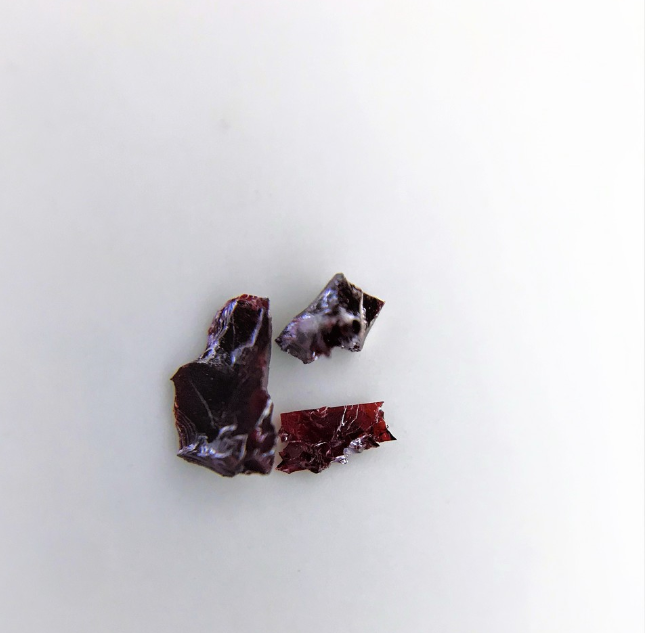

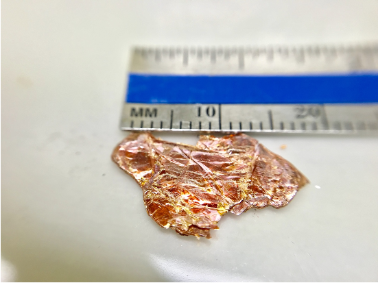
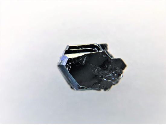
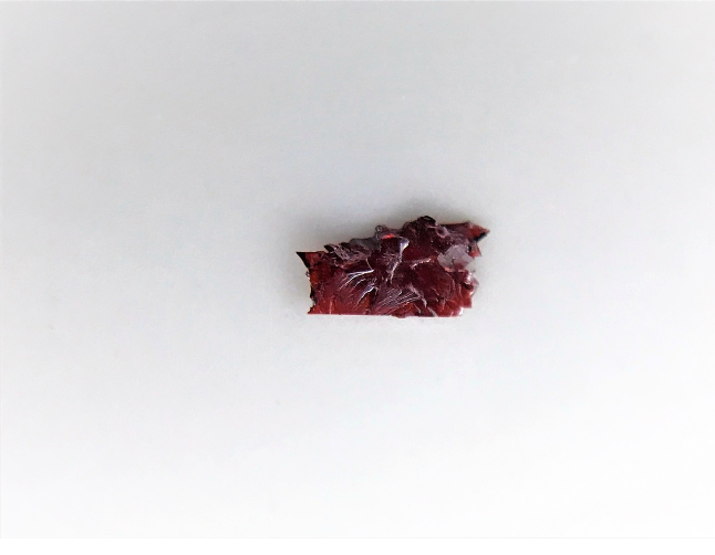
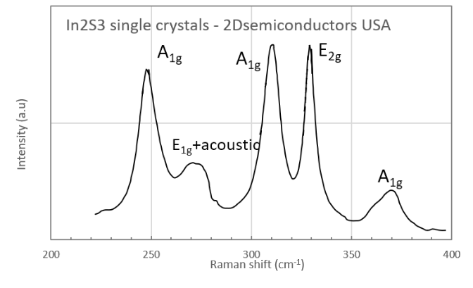
Gamma layered phase of In2S3 is a direct gap semiconductor with an optical band gap ranging from 2 eV - 3.25 eV. It's fundamental band gap nature (direct vs indirect) and its value have been much debaded in the field and remains open ended. In2S3 is particular attractive semiconductor for photoelectrochemical, solar cell, and photonic applications. Typical crystal sizes range in few-mm in size and each order contains 5-7 pieces of In2S3 crystals. The crystals appear layered but is harder to exfoliate compared to molybdenum disulfide. Thus, we recommend using highly adhesive tapes, ultrasonic exfoliation, or other methods to yield atomically thin sheets.

聯(lián)系人:嚴春偉
手機:13914543285
電話:0523-86190619,86192878
郵箱:taizhou@sunano.com.cn
地址: 江蘇省泰州市鳳凰西路168號